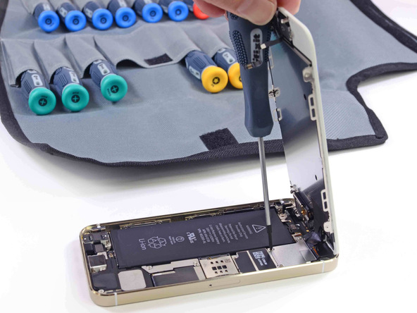
 It has been a tradition of iFixit, the immensely popular website known for its disassembling and assembling guides, to provide tear down images of Apple products as soon as they are launched. The Apple iPhone 5S is no exception and has received the tear down treatment from the website. The tear down has revealed some interesting details of the internal hardware that Apple never really reveals. The most important hardware addition to the iPhone 5S has been the fingerprint sensor. This is the Touch ID fingerprint sensor, after getting taken out of the device. According to iFixit, the TouchID fingerprint sensor is - A CMOS chip, the Touch ID is essentially a bunch of very small capacitors that creates an "image" of the ridges on your finger. This CMOS chip stores the images locally so that the data is not being sent over the networks, for privacy concerns of course. Here is how it look, from the inside of the iPhone 5S - Another change Apple have done, although minor, is the camera unit. The above image shows off the camera unit, with the codename - DNL333 41WGRF 4W61W, which is purportedly a Sony sensor again. It has been already revealed that the 8 Megapixel Sony ...
Source: http://www.fonearena.com/blog/82531/apple-iphone-5s-ifixit-tear-down-details-the-internals.html
